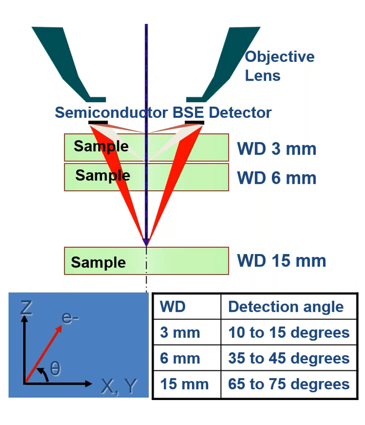

In just the last few years there has been a quantum leap in the ability of the scanning electron microscopes (SEMs and EPMAs) to observe and chemically analyze a wide variety of materials form various fields of interest and have drastically increased analysts’ capabilities.
However, these extremely low voltages come with some clearly defined sample preparation and handling procedures. Advances in X-ray spectroscopy, both in Energy Dispersive Spectroscopy (EDS) and a new novel Wavelength Dispersive Spectrometer (WDS) have also pushed the boundaries to higher mag, lower voltage and lower X-ray energy (soft X-ray) analysis opening up new avenues for specimen observation and analysis. These new state-of-the-art microscopes, detectors and spectrometers today allows one to overcome many of the historical limitations associated with low kV imaging and microanalysis.
HOWEVER, there are some considerations that may not have been thought about in the past. Some case studies and examples of the good things (and some of the bad) that can result from ultralow kV imaging and analysis will be presented. Ultra-low kV and or ultra-high spatial resolution is a VERY POWERFUL tool, and as with all powerful tools, it needs to be used with caution (or at least with keeping an eye out for the non-intuitive).
Who should attend?

Presenter: Vern Robertson, SEM Technical Sales Manager & EPMA / SA Product Manager
Vern has been with JEOL USA for 34 years. He was appointed EPMA/Surface Analysis Product Manager in 2016 and continues as SEM Technical Sales Manager, providing in-house and in the field, technical product support and customer applications support. Vern served as the senior SEM Applications Specialist at JEOL beginning in 1986. His prior industrial experience included eight years of consulting in an independent testing lab specializing in industrial and environmental problem solving, with responsibilities including polarized light optical microscopy, and atomic emission and absorption spectroscopy SEM with EDS/ WDS and X-ray diffraction.